

Microscopic methods
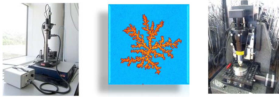
Atomic Force Microscope
Atomic Force Microscopy (AFM) is intended for determining the sample topography with a resolution of tenths of a nanometer in the vertical axis and up to units of nanometers in the lateral plane.
Two AFM microscopes are available in our department: Quesant Q-Scope 350 and NTegra Prima (NTMDT). In addition to the basic modes (contact and semi-contact), the NTegra allows measurements in other modes, including, among others: Scanning Tunneling Microscopy (STM) utilizing the tunneling current between the sample and the tip, Acoustic Force Allocation Microscopy (AFAM) for local measurement of hardness or Young's modulus, Kelvin Probe Microscopy, and electrical resistance measurement for mapping surface potential distribution and local currents, and more. Furthermore, the AFM microscope NTegra Prima can be combined with the Triboscope 75 nanoindenter (Hysitron) featuring the nano-DMAIII module. This setup overcomes the boundaries of current nanomechanical testing. The system enables dynamic mechanical analysis with a constant and variable oscillatory force superimposed on a precisely defined constant force, with variable frequency at a constant oscillatory force, and with a constant ratio between the constant and variable force components during the increase of the constant force. The application of a low oscillatory force allows for the measurement of even very thin layers, both soft and viscoelastic (polymers) and hard (metals, metal oxides).

Scanning Electron Microscope
For studying the morphology of nanomaterials, we have a JSM-7900F (JEOL) Scanning Electron Microscope available, which enables imaging the surface of samples with a resolution of up to 1 nm and the analysis of samples at pressures up to 400 Pa. The electron microscope is equipped with a wide range of detectors for both secondary and backscattered electrons, allowing for the comprehensive characterization of a variety of micro- and nanomaterials, including biological samples, with magnifications from 10x to 1,000,000x at electron beam energies in the range of 0.01 - 30 kV and a beam current from a few pA up to 500 nA.
The microscope is also equipped with a JED-2300 (JEOL) EDS detector, which allows for determining the elemental composition of the measured samples.

Profilometer
Stylus profilometry is a contact measurement method used to measure surface topography and material roughness. It operates on the principle of mechanical sensing: a diamond stylus with a very small tip radius moves at a constant speed across the measured surface, tracing its irregularities. The vertical movement of the stylus is sensed and converted into an electrical signal, which is used to record the surface profile—essentially, a height cross-section. In our department, we have the DEKTAK PRO stylus profilometer from Bruker, which enables a vertical resolution of 0.4 nm and 2D scanning of the surface of the studied materials.

