Scanning Electron Microscopy (SEM)
Scanning electron microscopy is nowadays a standard method for investigation of the structure of materials. Our SEM lab is equipped with two microscopes that allow the use of a wide range of analytical methods. Moreover, one of the microscopes is equipped with a focused ion beam (FIB), which enables sample preparation (cross-sections, TEM lamella preparation, 3D measurements) with the accuracy of tens of nanometers.
Both microscopes are equipped with a field emission gun (FEG) that provides the best available electron beam quality and both are equipped with standard detectors of secondary and backscattered electrons.
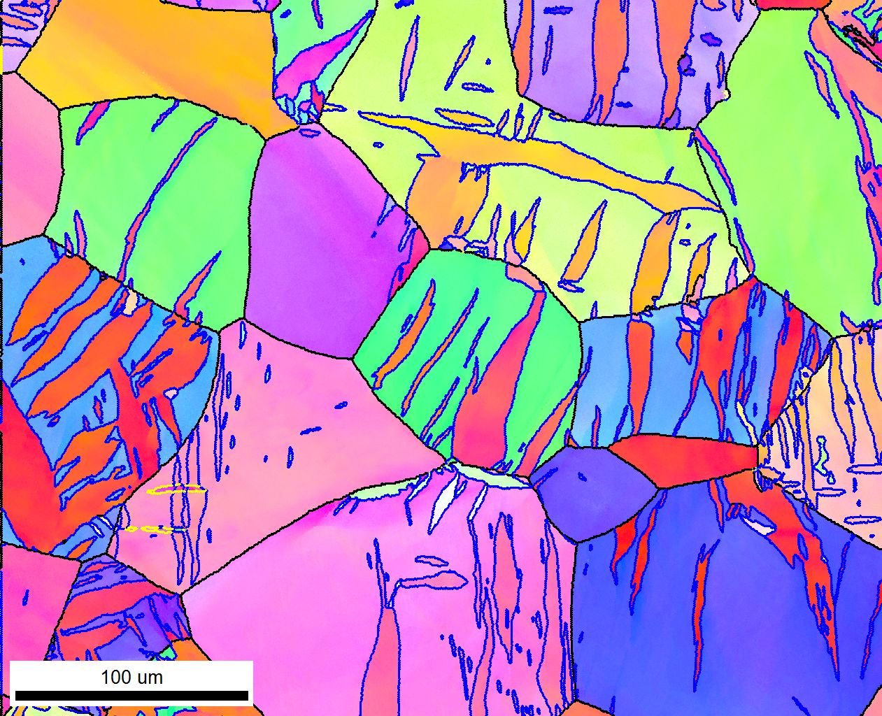
The microscopes are equipped with energy-dispersive X-ray detectors (EDS) for the determination of the chemical composition of samples and electron back-scattered detectors (EBSD) for determination of crystallographic orientation.
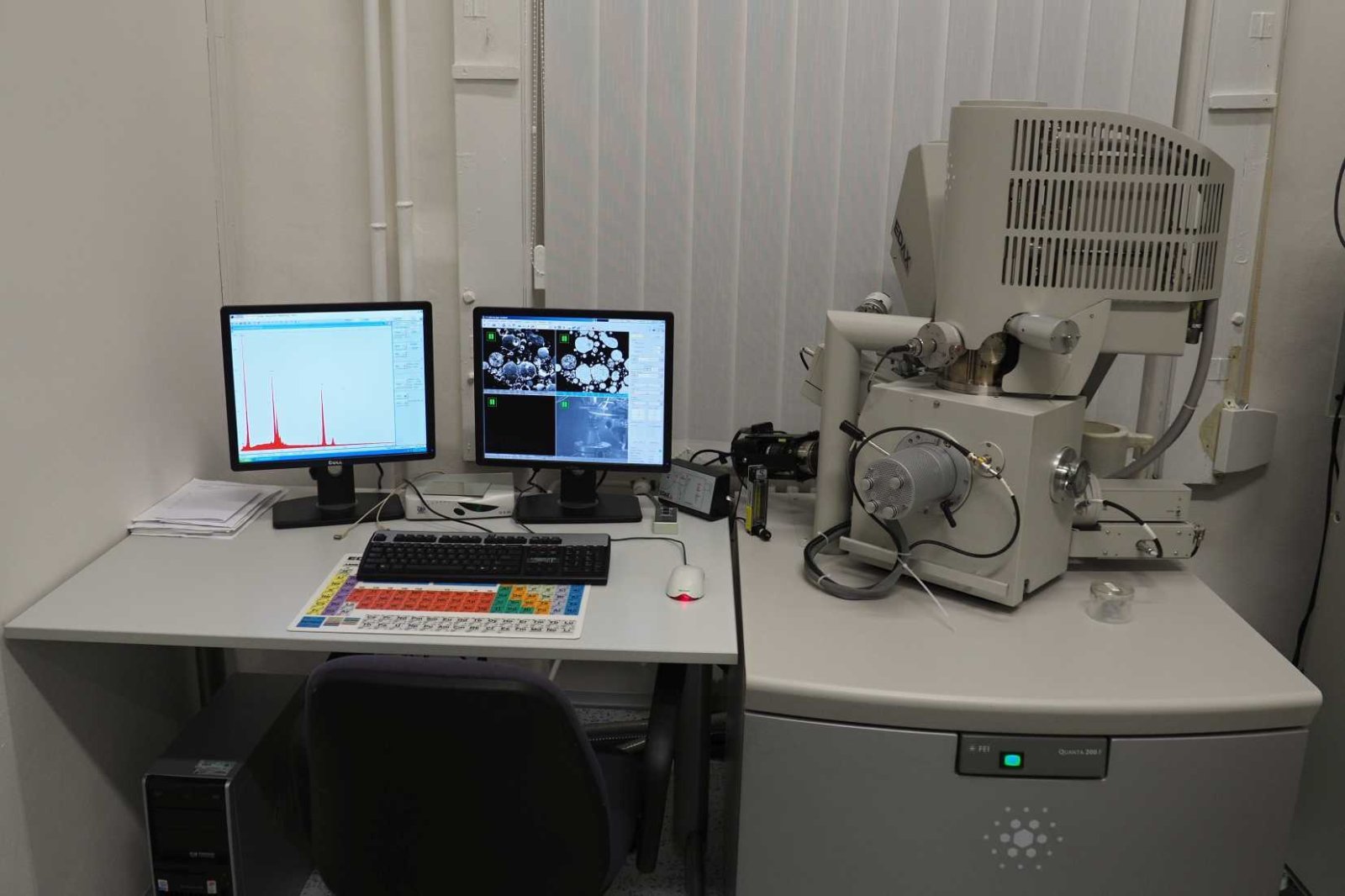
FEI Quanta 200F
This microscope is suitable for basic use for beginners (bachelor students) and for teaching. In addition to all of the detectors described above, this microscope is equipped with a wavelength-dispersive X-ray detector (WDS) enabling very precise analysis of chemical composition. The microscope also features a special mode for observations under reduced vacuum, which allows studies of non-conductive samples (including biological ones) without any modification.
Zeiss Auriga Compact
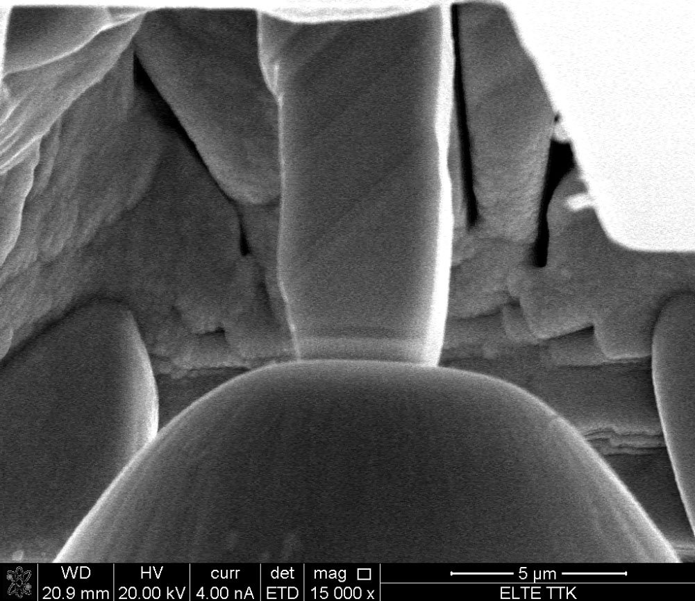
This microscope is used for more advanced analyses. It is equipped with a focused ion beam (FIB), which allows high precision sample milling. This enables us to study samples in 3D (by repeated milling and analyzing exposed layers of the material) with the accuracy of tens of nanometers or to produce samples for TEM from specific locations with the final thickness below 100 nm. Furthermore, a deformation and heating stage MTI SEMtester 1000 can be mounted into this microscope, which enables in-situ observation of material behavior during deformation and/or at elevated temperatures.
Contact: RNDr. Petr Harcuba, Ph.D.